- 您现在的位置:买卖IC网 > Sheet目录1998 > ICS844071AGLFT (IDT, Integrated Device Technology Inc)IC CLOCK GEN GIG ETH 8-TSSOP
ICS844071AG REVISION B OCTOBER 10, 2012
5
2012 Integrated Device Technology, Inc.
ICS844071 Data Sheet
FEMTOCLOCK CRYSTAL-TO-LVDS CLOCK GENERATOR
AC Electrical Characteristics
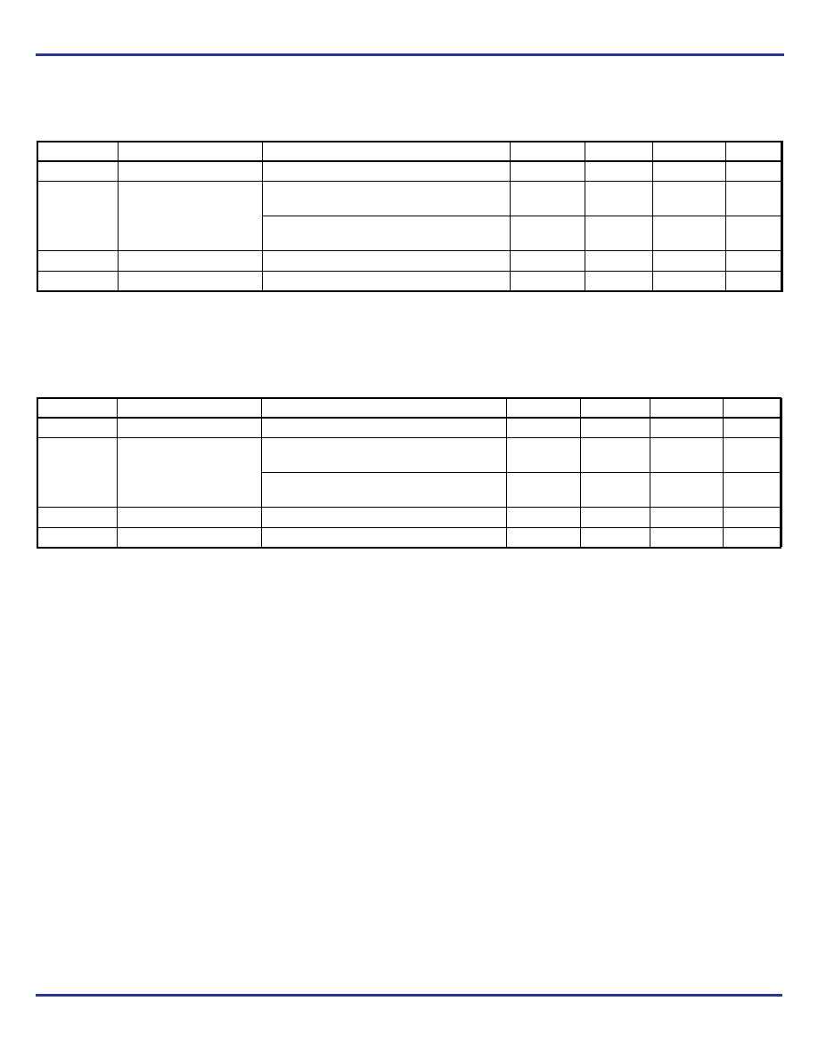
Table 5A. AC Characteristics, VDD = 3.3V ± 10%, TA = 0°C to 70°
NOTE: Electrical parameters are guaranteed over the specified ambient operating temperature range, which is established when the device is
mounted in a test socket with maintained transverse airflow greater than 500 lfpm. The device will meet specifications after thermal equilibrium
has been reached under these conditions. For additional information, refer to the PCI Express Application Note section in the datasheet.
NOTE 1: Refer to the Phase Noise Plot.
Table 5B. AC Characteristics, VDD = 2.5V ± 5%, TA = 0°C to 70°
NOTE: Electrical parameters are guaranteed over the specified ambient operating temperature range, which is established when the device is
mounted in a test socket with maintained transverse airflow greater than 500 lfpm. The device will meet specifications after thermal equilibrium
has been reached under these conditions. For additional information, refer to the PCI Express Application Note section in the datasheet.
NOTE 1: Refer to the Phase Noise Plot.
Parameter
Symbol
Test Conditions
Minimum
Typical
Maximum
Units
fOUT
Output Frequency
62.5
170
MHz
tjit()
RMS Phase Jitter,
Random; NOTE 1
150MHz,
Integration Range: 900kHz – 7.5MHz
0.45
ps
75MHz,
Integration Range: 900kHz – 7.5MHz
0.46
ps
tR / tF
Output Rise/Fall Time
20% to 80%
150
400
ps
odc
Output Duty Cycle
48
52
%
Parameter
Symbol
Test Conditions
Minimum
Typical
Maximum
Units
fOUT
Output Frequency
62.5
170
MHz
tjit()
RMS Phase Jitter,
Random; NOTE 1
150MHz,
Integration Range: 900kHz – 7.5MHz
0.56
ps
75MHz,
Integration Range: 900kHz – 7.5MHz
0.60
ps
tR / tF
Output Rise/Fall Time
20% to 80%
150
400
ps
odc
Output Duty Cycle
48
52
%
发布紧急采购,3分钟左右您将得到回复。
相关PDF资料
ICS844201BG-45LF
IC CLK GENERATOR 25MHZ 8TSSOP
ICS844204BK-245LF
IC CLK SYNTHESIZER 4LVDS 32VFQFN
ICS844S42BKILF
IC SYNTHESIZER RF FREQ 56-VFQFPN
ICS86004BG-01LF
IC CLK BUFFER ZD 1:4 16-TSSOP
ICS8634BY-01LFT
IC BUFFER ZD 1-5 LVPECL 32-LQFP
ICS8701AY-01LF
IC CLK GEN POLARITY CTRL 48-LQFP
ICS8701CYLF
IC CLK GENERATOR /1 /2 48-LQFP
ICS870931ARI-01LF
IC CLK GENERATOR LVCMOS 20QSOP
相关代理商/技术参数
ICS844201BG-45LF
功能描述:IC CLK GENERATOR 25MHZ 8TSSOP RoHS:是 类别:集成电路 (IC) >> 时钟/计时 - 专用 系列:HiPerClockS™, FemtoClock™, PCI Express® (PCIe) 标准包装:1,500 系列:- 类型:时钟缓冲器/驱动器 PLL:是 主要目的:- 输入:- 输出:- 电路数:- 比率 - 输入:输出:- 差分 - 输入:输出:- 频率 - 最大:- 电源电压:3.3V 工作温度:0°C ~ 70°C 安装类型:表面贴装 封装/外壳:28-SSOP(0.209",5.30mm 宽) 供应商设备封装:28-SSOP 包装:带卷 (TR) 其它名称:93786AFT
ICS844201BG-45LFT
功能描述:IC CLK GENERATOR 25MHZ 8TSSOP RoHS:是 类别:集成电路 (IC) >> 时钟/计时 - 专用 系列:HiPerClockS™, FemtoClock™, PCI Express® (PCIe) 标准包装:1,500 系列:- 类型:时钟缓冲器/驱动器 PLL:是 主要目的:- 输入:- 输出:- 电路数:- 比率 - 输入:输出:- 差分 - 输入:输出:- 频率 - 最大:- 电源电压:3.3V 工作温度:0°C ~ 70°C 安装类型:表面贴装 封装/外壳:28-SSOP(0.209",5.30mm 宽) 供应商设备封装:28-SSOP 包装:带卷 (TR) 其它名称:93786AFT
ICS844201BGI-45LF
功能描述:IC CLK GENERATOR 25MHZ 8TSSOP RoHS:是 类别:集成电路 (IC) >> 时钟/计时 - 专用 系列:HiPerClockS™, FemtoClock™, PCI Express® (PCIe) 标准包装:1,500 系列:- 类型:时钟缓冲器/驱动器 PLL:是 主要目的:- 输入:- 输出:- 电路数:- 比率 - 输入:输出:- 差分 - 输入:输出:- 频率 - 最大:- 电源电压:3.3V 工作温度:0°C ~ 70°C 安装类型:表面贴装 封装/外壳:28-SSOP(0.209",5.30mm 宽) 供应商设备封装:28-SSOP 包装:带卷 (TR) 其它名称:93786AFT
ICS844201BGI-45LFT
功能描述:IC CLK GENERATOR 25MHZ 8TSSOP RoHS:是 类别:集成电路 (IC) >> 时钟/计时 - 专用 系列:HiPerClockS™, FemtoClock™, PCI Express® (PCIe) 标准包装:1,500 系列:- 类型:时钟缓冲器/驱动器 PLL:是 主要目的:- 输入:- 输出:- 电路数:- 比率 - 输入:输出:- 差分 - 输入:输出:- 频率 - 最大:- 电源电压:3.3V 工作温度:0°C ~ 70°C 安装类型:表面贴装 封装/外壳:28-SSOP(0.209",5.30mm 宽) 供应商设备封装:28-SSOP 包装:带卷 (TR) 其它名称:93786AFT
ICS844202AK-245LF
功能描述:IC CLOCK GEN SRL SCSI 32-VFQFPN RoHS:是 类别:集成电路 (IC) >> 时钟/计时 - 专用 系列:HiPerClockS™, PCI Express® (PCIe) 标准包装:28 系列:- 类型:时钟/频率发生器 PLL:是 主要目的:Intel CPU 服务器 输入:时钟 输出:LVCMOS 电路数:1 比率 - 输入:输出:3:22 差分 - 输入:输出:无/是 频率 - 最大:400MHz 电源电压:3.135 V ~ 3.465 V 工作温度:0°C ~ 85°C 安装类型:表面贴装 封装/外壳:64-TFSOP (0.240",6.10mm 宽) 供应商设备封装:64-TSSOP 包装:管件
ICS844202AK-245LFT
功能描述:IC CLOCK GEN SRL SCSI 32-VFQFPN RoHS:是 类别:集成电路 (IC) >> 时钟/计时 - 专用 系列:HiPerClockS™, PCI Express® (PCIe) 标准包装:28 系列:- 类型:时钟/频率发生器 PLL:是 主要目的:Intel CPU 服务器 输入:时钟 输出:LVCMOS 电路数:1 比率 - 输入:输出:3:22 差分 - 输入:输出:无/是 频率 - 最大:400MHz 电源电压:3.135 V ~ 3.465 V 工作温度:0°C ~ 85°C 安装类型:表面贴装 封装/外壳:64-TFSOP (0.240",6.10mm 宽) 供应商设备封装:64-TSSOP 包装:管件
ICS844202AKI-245LF
功能描述:IC CLOCK GEN SRL SCSI 32-VFQFPN RoHS:是 类别:集成电路 (IC) >> 时钟/计时 - 专用 系列:HiPerClockS™, PCI Express® (PCIe) 标准包装:1,500 系列:- 类型:时钟缓冲器/驱动器 PLL:是 主要目的:- 输入:- 输出:- 电路数:- 比率 - 输入:输出:- 差分 - 输入:输出:- 频率 - 最大:- 电源电压:3.3V 工作温度:0°C ~ 70°C 安装类型:表面贴装 封装/外壳:28-SSOP(0.209",5.30mm 宽) 供应商设备封装:28-SSOP 包装:带卷 (TR) 其它名称:93786AFT
ICS844202AKI-245LFT
功能描述:IC CLOCK GEN SRL SCSI 32-VFQFPN RoHS:是 类别:集成电路 (IC) >> 时钟/计时 - 专用 系列:HiPerClockS™, PCI Express® (PCIe) 标准包装:28 系列:- 类型:时钟/频率发生器 PLL:是 主要目的:Intel CPU 服务器 输入:时钟 输出:LVCMOS 电路数:1 比率 - 输入:输出:3:22 差分 - 输入:输出:无/是 频率 - 最大:400MHz 电源电压:3.135 V ~ 3.465 V 工作温度:0°C ~ 85°C 安装类型:表面贴装 封装/外壳:64-TFSOP (0.240",6.10mm 宽) 供应商设备封装:64-TSSOP 包装:管件